Large Area Defect Mapping Instrument & High Resolution Defect Mapping Instrument
SE20 & SE21
If the glass is not thoroughly cleaned, or if there is dust in the chamber, causing holes in perovskite crystallization and thereby reducing PSC efficiency, how can this be quickly detected?
To address this, we introduce
two fast and efficient solutions—SE20 and SE21
—to help customers quickly detect perovskite crystallization defects (pinholes and voids) caused by
uncleaned glass or chamber dust
.
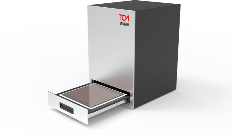
SE20
Large Area Defect Mapping Instrument
· High Precision: 60μm per pixel resolution
· Large Scan Area: 250×250mm coverage
· Smart Analysis: Automatic pinhole size statistics
· Automatic Sorting: Custom defect criteria for reject screening

SE21
High Resolution Defect Mapping Instrument
· Micro-Scale Resolution: Detect defects as small as 5μm
· Focused Inspection Area: 2×2mm high-magnification observation
· Multi-Point Scanning: Motorized stage enables efficient sample mapping
· Smart Analysis: Void size distribution statistics
 Shenzhen TDM Technology Co., Ltd.
8th Floor, Unit C039, Meili AAA Commercial Building, No. 428 Jinglong Zhonghuan Road, Longyuan Community, Longhua Street, Longhua District, Shenzhen, China, 518109.
Suzhou TDM Technology Co., Ltd.
Pioneer Park-Building No. 4, ZhuYuan Road 209, HuQiu District, Suzhou, Jiangsu Province, China, 215129.
 E-mail:charlie@tdm-tek.com
 Wechat