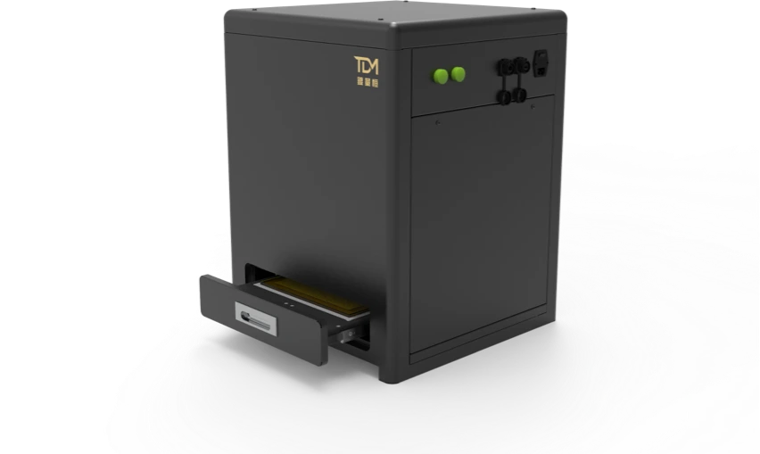
EL/PL&Defect Mapping Instrument
SE60
Struggling with laser scribing defects or crystallization issues in perovskite production?
The SE60 delivers fast, reliable answers!
The SE60 delivers fast, reliable answers!
Validated by industry partners
solves real-world production challenges
Precision detection
laser scribing irregularities and crystal defects
Trusted solution
already enhancing quality control for leading manufacturers
Key Features

Industry First:
The world's first EL/PL mapping integrated system for perovskite-based solar cell sorting and defect analysis.

Patented Technology:
Combines EL mapping, PL mapping, and AI capabilities for precise multi-defect analysis.

Single Scan:
Eliminates misalignment and brightness variation with one-time imaging.

Professional Service:
Beyond just EL/PL imaging—we provide expert recommendations based on results to support R&D and production decisions.
 Shenzhen TDM Technology Co., Ltd.
8th Floor, Unit C039, Meili AAA Commercial Building, No. 428 Jinglong Zhonghuan Road, Longyuan Community, Longhua Street, Longhua District, Shenzhen, China, 518109.
Suzhou TDM Technology Co., Ltd.
Pioneer Park-Building No. 4, ZhuYuan Road 209, HuQiu District, Suzhou, Jiangsu Province, China, 215129.
 E-mail:charlie@tdm-tek.com
 Wechat