Inline EL/PL mapping metrology solution
SE6000
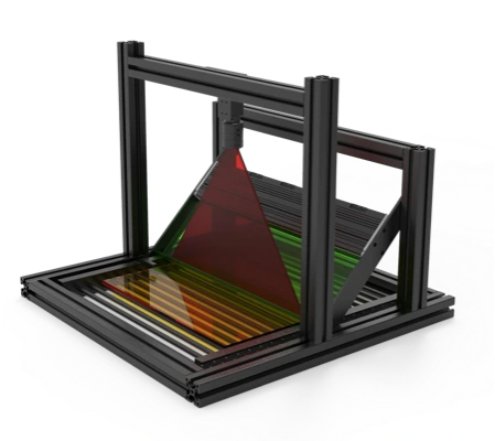
Full-Panel EL/PL Imaging for Smarter Perovskite Production
Uncover every critical detail with our
automated EL/PL mapping solution
:
✔ Whole-panel imaging – Capture every cm² of perovskite films or finished modules
✔ AI-powered defect classification – Instantly identify:
• Absorption layer irregularities
• Electrode flaws
• Laser scribing defects
• Micro-shorts & current leakage points
✔ Whole-panel imaging – Capture every cm² of perovskite films or finished modules
✔ AI-powered defect classification – Instantly identify:
• Absorption layer irregularities
• Electrode flaws
• Laser scribing defects
• Micro-shorts & current leakage points
Key Benefits
Seamless integration with
existing production lines
existing production lines
Quantitative quality scoring for
every production batch
every production batch
100% area inspection
vs
traditional sampling
vs
traditional sampling
 Shenzhen TDM Technology Co., Ltd.
8th Floor, Unit C039, Meili AAA Commercial Building, No. 428 Jinglong Zhonghuan Road, Longyuan Community, Longhua Street, Longhua District, Shenzhen, China, 518109.
Suzhou TDM Technology Co., Ltd.
Pioneer Park-Building No. 4, ZhuYuan Road 209, HuQiu District, Suzhou, Jiangsu Province, China, 215129.
 E-mail:charlie@tdm-tek.com
 Wechat