TDM Technology

About Us

TDM TECHNOLOGY

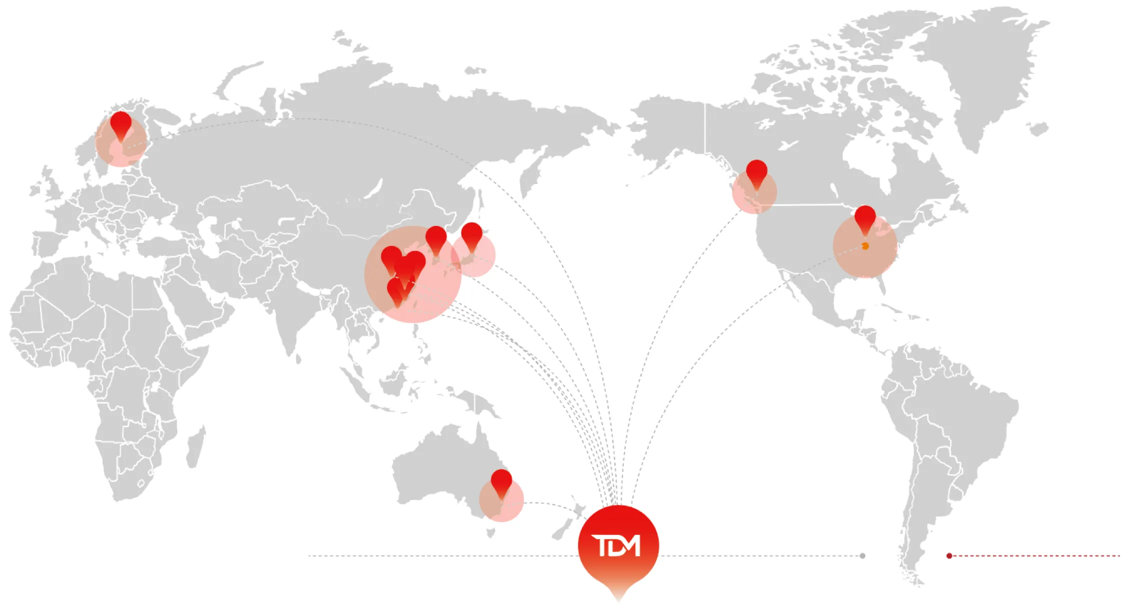
Founded in 2023, TDM Technology (legal name: Suzhou TDM Technology Co., Ltd.) is headquartered in Suzhou, China, with a Shenzhen branch. Regional partners support marketing and after-sales in the United States (TECHCESS SOLUTIONS LLC), Germany (JKY Business Solutions GmbH), the United Kingdom (X&X TECHNOLOGY LTD) and Japan (昌富産業株式会社). We specialize in high-precision thin film measurement equipment. Guided by first-principles thinking, we pioneer non-destructive testing technologies to break technical barriers. We provide comprehensive offline, inline, and in-situ inspection solutions for strategic industries like photovoltaics, semiconductors, and advanced displays.

Recognized supplier on Thomasnet — view our profile: TDM Technology Co., Ltd. on Thomasnet

Core R&D Team: Composed of senior physicists and optical engineers with backgrounds from CAS and overseas labs. The core R&D team has 20+ years of experience, covering the full spectrum from material R&D and prototyping to mass production deployment.

Leveraging deep expertise in physics and optics, TDM delivers stable, high-precision, closed-loop measurement solutions for the new energy, semiconductor, and display industries. We drive technological innovation to enhance quality, yield, and intelligent manufacturing for our partners.

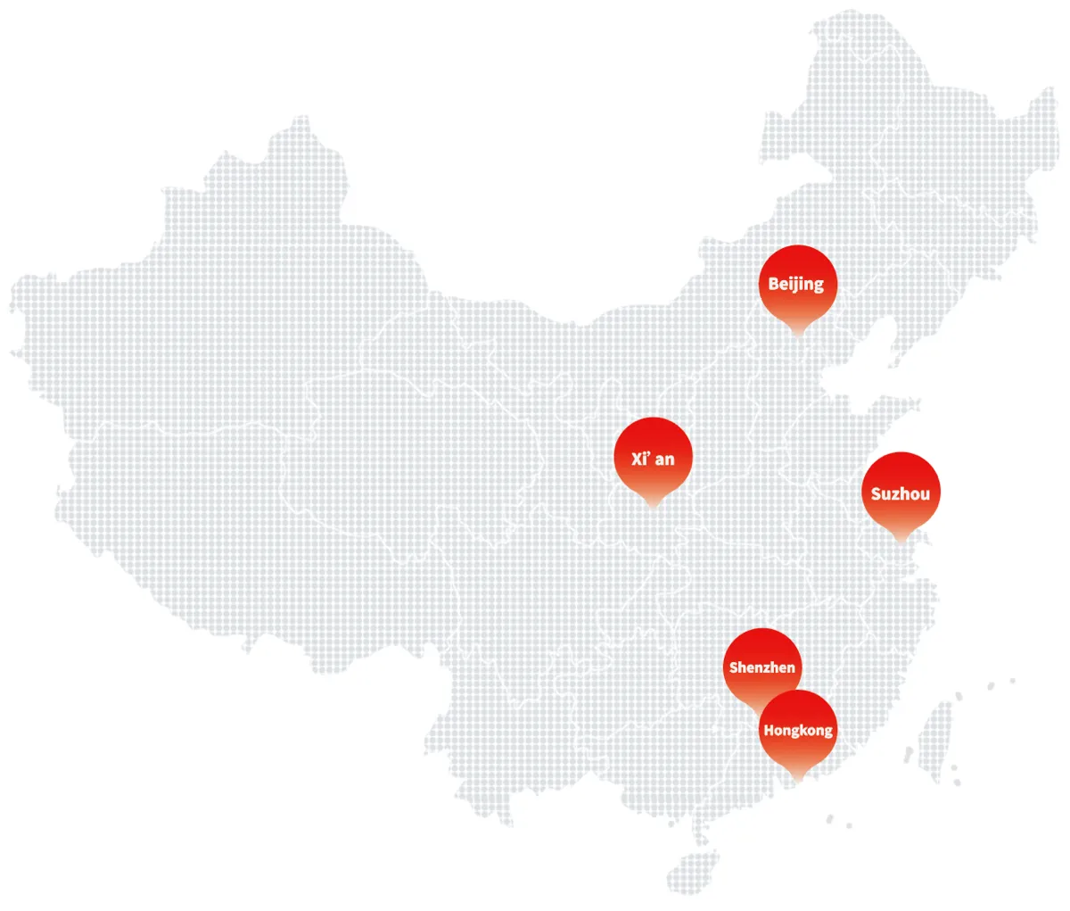
TDM Technology global locations: Suzhou, Shenzhen, Beijing, Xi'an, Hong Kong, San Francisco and Dallas
TDM Technology headquarters in Suzhou
10+
Self-owned Patents
2023
Year Founded
50%
R&D Personnel
50+
Partner Organizations
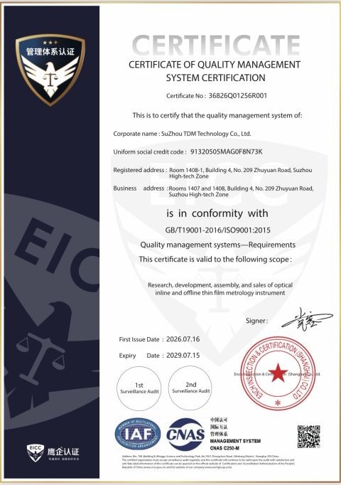
ISO 9001
Quality System
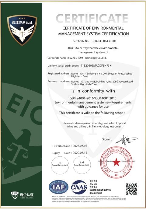
ISO 14001
Environment System

TDM is a high-tech company specializing in the development of advanced thin film metrology equipment and solutions;

We leverage first principles as the foundation for innovation, revolutionizing thin film coating metrology technologies to effectively address the needs of customers in industries such as semiconductors, renewable energy, and displays.

  • Focused on Thin Film Metrology technology and solutions;
  • Serve semiconductor, renewable energy, and display industries;
  • A team of senior physicists, optical and electrical engineers
ISO 9001:2015 Quality Management System certificate, No. 36826Q01256R001, issued by Ench Inspection & Certification (Shanghai) Co., Ltd., valid through 15 July 2027

No. 36826Q01256R001 · Valid through 15 Jul 2027

ISO 14001:2015 Environmental Management System certificate, No. 36826E00643R001, issued by Ench Inspection & Certification (Shanghai) Co., Ltd., currently certified

No. 36826E00643R001 · Currently certified

Patents

A Method and Apparatus for Measuring Thin-Film Thickness on Textured Silicon Substrates

  • Patent No.: ZL 2024 1 1744025.2
  • Publication No.: CN 119594868 B
  • Jurisdiction: China
  • Status: Granted
  • Filed: November 30, 2024
  • Granted: November 21, 2025

Protects a method and apparatus for measuring thin-film thickness on textured silicon substrates — supporting TDM's optical metrology used in PV and semiconductor film inspection.

Core Advantages

Full Scenario Coverage

Covers offline laboratory equipment, inline production line integration, and two in-situ monitoring routes. SE31 and SE310 monitor film thickness and reflectance from the coating head. SE31-FM provides a separate wide-band transmission/reflection optical-film monitoring route; specifications are model-specific.

Multi-Industry Adaptability

Versatile for PV, semiconductor, display panels, optical coatings, and new energy. Supports multi-layer composite films, metal/dielectric/ITO layer detection.

Self-Developed Core Technology

Published systems cover optical film thickness, reflectance, transmittance, n/k, band gap, PL, mapping and 3D profiling. Measurement range, repeatability and sampling mode are specified by model.

One-Stop Service

Complete set of services including equipment, line integration, software, on-site calibration, and lifetime after-sales technical support.

Industry Recognition & Speaking Engagements

4 June 2026

SNEC International Pioneer Perovskite Forum 2026

Charlie Chen, General Manager of Suzhou TDM Technology Co., Ltd., was invited to speak at the SNEC International Pioneer Perovskite Forum 2026 on “No Metrology, No Scale — Inline Metrology and AI Empowering Intelligent Perovskite Manufacturing.”

View SNEC Forum Program

R&D and Technical Strength

  • 10+ self-owned thin film measurement patents
  • 50% of personnel work in R&D
  • Core R&D team with 20+ years of experience
  • Offline, inline and in-situ product configurations
R&D and technical strength

Our Customers

Our global customers

Connect With Us

Follow TDM Technology on LinkedIn for company updates, product news and industry events.

LinkedIn — Suzhou TDM Technology Co., Ltd.

We publish field notes and quick-reference tables on our Thin Film Metrology Reference repository.

Our Team

Our core R&D team consists of senior physicists and optical engineers from the Chinese Academy of Sciences and overseas laboratories, with 20+ years of experience spanning material research, equipment development, and mass-production deployment.

Deep professional background

Rich engineering experience

From world-class universities

Partner universities and research institutes