

Core Applications
For lenses, mirrors, and prisms: precise roughness, form accuracy (PV/RMS), and radius of curvature across core optics manufacturing steps.
Anti-reflection (AR) coating: 100 nm - 300 nm, Quarter-wave thickness control for minimum reflectance
Polarizer / polarizing film: 10 um - 50 um, Ensures polarization efficiency and image uniformity
Organic emissive & functional layers: 10 nm - 200 nm, Organic layer thickness directly affects brightness and lifetime
For lenses, mirrors, and prisms: precise roughness, form accuracy (PV/RMS), and radius of curvature across core optics manufacturing steps.

White-light interferometry (WLI) enables non-contact, nanoscale 3D topography—suited to complex freeform surfaces of optical components.

Mount on a precision isolation stage; high-magnification point scans plus analysis software auto-extract form error into a full metrology report.

Ensures imaging quality meets design specs; traces form errors to root causes for grinding/polishing/coating optimization and higher yield.
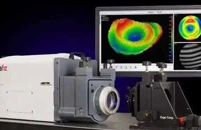
The system captures data in real time and builds color form-error maps—showing nanoscale surface detail on lenses, prisms, and more.
Anti-reflection (AR) coatings are typically 100–300 nm and need quarter-wave thickness for minimum reflectance. Polarizer films (10–50 µm) affect polarization efficiency and image uniformity. OLED evaporation of organic emissive and functional layers (10–200 nm) controls brightness and lifetime. Lenses, mirrors and prisms also need roughness, form accuracy (PV/RMS) and radius of curvature.
A quarter-wave optical thickness at the design wavelength produces destructive interference in reflection. Drift of even tens of nanometers in a 100–300 nm AR stack raises residual reflectance and hurts imaging contrast, so non-contact thickness metrology is used during coating.
White-light interferometry (WLI) provides non-contact, nanoscale 3D topography suited to complex freeform surfaces. A typical workflow mounts the part on a precision isolation stage, runs high-magnification point scans, and lets analysis software extract form error into a full metrology report.
Real-time color form-error maps show nanoscale surface detail on lenses and prisms. Tracing PV/RMS errors back to grinding, polishing or coating steps lets the process be corrected so imaging quality meets design specs and yield rises.
