

Core Applications
Glovebox monitoring of perovskite crystallization.Thickness after spin-coat; defects after coating and encapsulation.In-line thickness & PL, real time defect checks, plus pre-shipment stability and electrical safety tests.

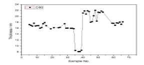
Buffer layers (NiOx, SnO₂, TiO₂, C60): 10 nm - 100 nm, Carrier transport efficiency; thickness deviation impacts device performance
Silicon thin films (a-Si, uc-Si): 100 nm - 3 um, Controls spectral absorption across wavelength bands
Perovskite wet / semi-dry / dry films: 10 nm - 1 um, Full-stack metrology for in-line monitoring and closed-loop feedback
Transparent conductive oxides (FTO, ITO, IWO): 200 nm - 1 um, Affects transmittance and conductivity—key efficiency parameters
Full stack: CdS window, CdTe absorber, back contact (e.g. ZnTe:Cu): 10 nm - 8 um, Full-stack thickness control impacts Voc and conversion efficiency; boosts process yield
Full stack: Mo back contact, CIGS absorber, CdS buffer, ZnO:Al window: 30 nm - 2.5 um, Full-stack metrology—each layer thickness is critical for absorption, carrier transport and efficiency; enables closed-loop line control
Glovebox monitoring of perovskite crystallization.Thickness after spin-coat; defects after coating and encapsulation.In-line thickness & PL, real time defect checks, plus pre-shipment stability and electrical safety tests.

Non-contact interferometry delivers nanoscale thickness metrology without surface damage—enabling fast inspection.

Multi-point auto-scan of the module surface; real-time data capture with auto calculation of thickness uniformity and average PL.

Real-time monitoring ensures that the film thickness and PL remain within the process range. It promptly provides feedback and adjusts the process parameters, effectively avoiding defects and significantly improving the overall yield of component manufacturing.
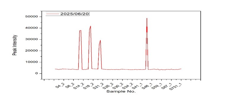
In-line test view: film thickness and PL trends, with anomaly detection highlighted.
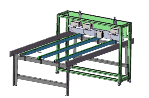
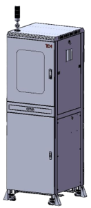
Typical stacks include interface transport layers such as NiOx, SnO₂, TiO₂ and CoO (10–100 nm); silicon absorbers a-Si and µc-Si (100 nm–3 µm); perovskite wet, semi-dry and dry films (10 nm–1 µm); and transparent electrodes FTO, ITO and IWO (200 nm–1 µm). CdTe and CIGS full stacks also require layer-by-layer thickness control because each layer affects Voc, absorption and conversion efficiency.
In-line systems measure thickness and photoluminescence (PL) together—bandgap, peak and FWHM—plus defects after coating and encapsulation. Glovebox monitoring of crystallization, real-time thickness/PL and pre-shipment stability and electrical-safety tests form a full-stack metrology loop for closed-loop process feedback.
CdTe stacks (CdS window, CdTe absorber, back contact such as ZnTe:Cu, 10 nm–8 µm) and CIGS stacks (Mo, CIGS, CdS, ZnO:Al, 30 nm–2.5 µm) only deliver design efficiency when every layer is in spec. Measuring the full stack enables closed-loop line control instead of catching a bad absorber after the module is finished.
Multi-point auto-scan of the module surface reports thickness uniformity and average PL in real time. Keeping both thickness and PL inside the process window, with fast parameter feedback, reduces coating defects and raises module manufacturing yield.
