

Pain Points: Limits of Traditional Methods
End-of-line sampling cannot cover 100%; delayed feedback blocks real-time correction and precise defect tracing.

Organic Emissive Material Film: 20 nm – 80 nm, Thickness directly determines luminous efficiency, color coordinates and device lifetime; sub-nm precision control is critical for uniform display image quality.
Amorphous Indium Gallium Zinc Oxide (a-IGZO) Film: 30 nm – 100 nm, Thickness uniformity governs TFT switching characteristics and panel pixel-to-pixel consistency; in-line monitoring directly correlates with production yield.
Indium Tin Oxide (ITO) Film: 20 nm – 150 nm, Thickness balances sheet resistance and optical transmittance; real-time metrology optimizes the trade-off between touch sensitivity and display brightness.
End-of-line sampling cannot cover 100%; delayed feedback blocks real-time correction and precise defect tracing.

Non-contact optical sensing between slot die head and pre-bake enables continuous, non-destructive wet-film inspection in process.

Millisecond feedback enables instant tuning with zero miss risk; pinpoint defects, cut waste, and raise yield and cost efficiency.
In-situ module after the slot die head, linked to MES for millisecond thickness monitoring—stopping coating defects at the source.
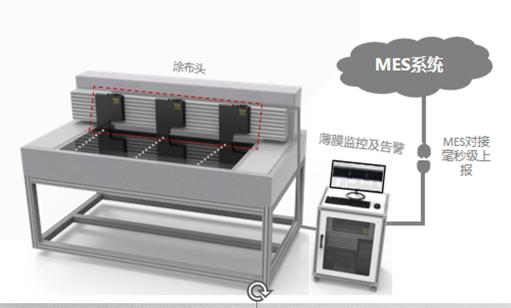
Broadband thin-film interferometry captures wet-film optics. Custom hardware and algorithms deliver non-contact, high-precision, real-time monitoring.
Filters stray light in wet-film optics for high SNR and clean signals.
Fits tight line spaces, cuts path loss, boosts vibration immunity.
Tiny spot captures local thickness at micron-level resolution.
Local real-time analysis for ms response and closed-loop control.
Organic emissive films are typically 20–80 nm. Thickness sets luminous efficiency, color coordinates and lifetime; small deviations show up as panel non-uniformity. Sub-nanometer control is required for a uniform display image.
Amorphous IGZO active layers are typically 30–100 nm. Thickness uniformity governs TFT switching and pixel-to-pixel consistency, so in-line monitoring correlates directly with panel yield. End-of-line sampling cannot cover 100% of the glass and is too late for real-time correction.
ITO films in the 20–150 nm range must balance sheet resistance and optical transmittance. Real-time metrology is used to keep touch sensitivity without sacrificing display brightness.
Non-contact optical sensing between the slot-die head and pre-bake inspects wet film continuously. Broadband thin-film interferometry, a compact short optical path, a micron-scale spot and on-edge computing give millisecond thickness feedback into MES so coating defects are stopped at the source.
