

Core Applications
Covers post-CMP roughness, film thickness uniformity, etch-depth analysis, and high-precision 3D critical dimensions for MEMS.
Photoresist: 100 nm - 10 um, Controls lithography pattern accuracy and impacts chip yield
Dielectric films (SiO₂, Si₃N₄): 10 nm - 1 um, Gate oxide layer, interlayer dielectric; determines electrical performance of devices
Polyimide (PI) / UV coating: 5 um - 50 um, FPC insulating protective layer; thickness affects flexibility and reliability
Covers post-CMP roughness, film thickness uniformity, etch-depth analysis, and high-precision 3D critical dimensions for MEMS.

Non-contact white-light interferometry enables nanoscale 3D topography without wafer damage—meeting strict semiconductor process needs.

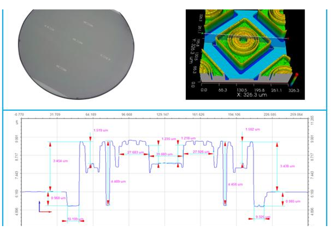
Multi-point auto-scan of the wafer; real-time capture with auto Sa/Sq roughness and film thickness uniformity (TTV) metrics.

Real-time control keeps Ra < 0.1 nm, feeds back process tweaks, suppresses defects, and significantly raises chip yield.
Wafer surface inspection flow: silicon wafer, 3D topography scan, and key profile metrics—showing micro-morphology analysis.
TDM metrology covers photoresist (typically 100 nm–10 µm) that controls lithography pattern accuracy and yield; dielectric films such as SiO₂ and Si₃N₄ (10 nm–1 µm) used as gate oxide and interlayer insulation; and polyimide or UV coatings (5–50 µm) that protect flexible circuits. Post-CMP roughness, thickness uniformity, etch depth and MEMS 3D critical dimensions are also in scope.
Photoresist thickness in the 100 nm–10 µm range controls pattern transfer accuracy. If the film is too thick or too thin, CD (critical dimension) drifts and chip yield drops. Non-destructive optical measurement verifies the resist before exposure without damaging the wafer.
Non-contact white-light interferometry maps nanoscale 3D topography without touching the wafer, which meets semiconductor process rules that forbid mechanical probes on product wafers. The same non-contact approach is used for dielectric thickness and post-CMP roughness.
Multi-point auto-scan captures Sa/Sq roughness and film-thickness uniformity (TTV) in real time. Closed-loop feedback is used to keep Ra below 0.1 nm, suppress defects and raise chip yield compared with offline sampling alone.
