

Current Challenges
Thin film deposition thickness is estimated empirically or theoretically.Excess deposition leads to wasted time and coating materials; insufficient deposition time results in inadequate film thickness.

Conformal coating: 3 um - 70 um, Moisture-, mold- and salt-fog protection for harsh-environment reliability
PVD/CVD functional films (e.g. DLC): 50 nm - 5 um, Wear layers for phone mid-frames/watch cases; thickness affects durability and appearance
Thin film deposition thickness is estimated empirically or theoretically.Excess deposition leads to wasted time and coating materials; insufficient deposition time results in inadequate film thickness.

Real-time monitoring of thin film thickness during coating process.Compliance reminder & alarm function available.Improve coating efficiency on production lines and save raw materials.
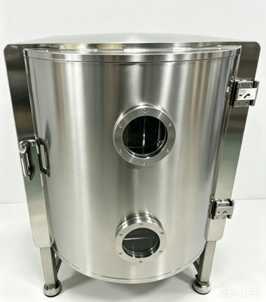


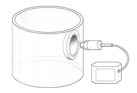
Conformal coatings on PCBs are typically 3–70 µm and provide moisture, mold and salt-fog protection. PVD/CVD functional films such as DLC on phone mid-frames and watch cases are typically 50 nm–5 µm; thickness affects both wear life and appearance.
When thickness is only estimated from time or theory, excess deposition wastes cycle time and coating material, while too short a deposition leaves the film under-spec. Real-time thickness monitoring with compliance alarms replaces that guesswork.
Measuring film thickness during coating, with limit reminders and alarms, lets the line stop at the target thickness. That raises coating efficiency and cuts raw-material use compared with over-depositing “to be safe.”
Yes. The same non-contact optical approach used on consumer housings applies to industrial protection films—for example flanges and observation ports—where wear or barrier thickness must stay in spec without damaging the coated surface.
